Keisuke Yamane

Associate Professor, Graduate School of Engineering, Toyohashi University of Technology*Profile is at the time of the award.

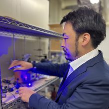
2025Inamori Research GrantsScience & Engineering

Research topics
Growth of Germanium co-doped with group-III and group-V elements for Silicon Photonics Application
Keyword
Summary
In recent years, rapid advancements in the field of silicon photonics have enabled the fabrication of various optical devices, excluding light-emitting elements, on Si substrates. This progress has facilitated the integration of sensors and optical communication functions onto a single chip. The final key device required is a light-emitting element compatible with the CMOS process.

The applicant has developed a technology for monolithic integration of light-emitting devices and LSI. However, due to material constraints, the realization of an infrared light source for optical communication has not yet been achieved. This study aims to establish a true monolithic integration technology by developing a novel infrared light-emitting material compatible with the CMOS process.

Existing materials such as InGaAs, GeSn, and n-Ge have yet to show a clear path toward system integration. Therefore, instead of following conventional materials, this research will explore new materials highly compatible with Si integrated circuits. Specifically, we will develop an alloying technology for III-V compound semiconductors and Ge, evaluate their electrical and optical properties, and aim to fabricate a light-emitting device.

The successful achievement of this research goal is expected to bring innovation to silicon photonics by enabling inter-chip optical communication without relying on external light sources, diverging from conventional approaches.

Comment

This research challenges the realization of a CMOS-compatible infrared light-emitting device, the final hurdle in the field of silicon photonics. Instead of relying on conventional materials, we adopt a unique approach by developing a mixed-crystal technology combining III-V compound semiconductors and Ge, paving the way for novel material exploration. Through this endeavor, we aim to establish true monolithic integration technology and bring innovation to silicon photonics. We are fully committed to ensuring the success of this research, laying the foundation for next-generation high-performance, low-power optical communication technology.

Find other recipients

Science & Engineering